[ 產品資訊 ] Machine Vision Microscopes
Metallography, or more recently materialography (metals plus composites), is the qualitative and quantitative description of the microstructure of metallic materials using microscopic methods. To be able to examine the microstructure under a light microscope, the workpiece must be prepared accordingly in advance. Small pieces must be separated from large components, embedded in a resin, and then ground, polished and, depending on the application, etched. Manufacturers of equipment for specimen preparation are e.g. Struers, QATM, Buehler, Leco, and many more.
These ground-glass samples are opaque to light and must therefore be examined in reflected light in order to detect the smallest defects and features through the interaction of the surface and the light irradiation used.
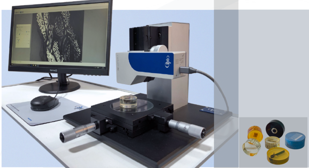
In reflected-light microscopy, a distinction is made between bright-field and dark-field illumination. In a pure digital microscope, the eyepiece is replaced by a camera chip, as in the imaging module of the compact M platform shown here.
In the quality assurance of metallic components, the assessment of damage cases based on material failure or in the development of new materials, these samples are examined and documented with a microscope.
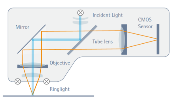
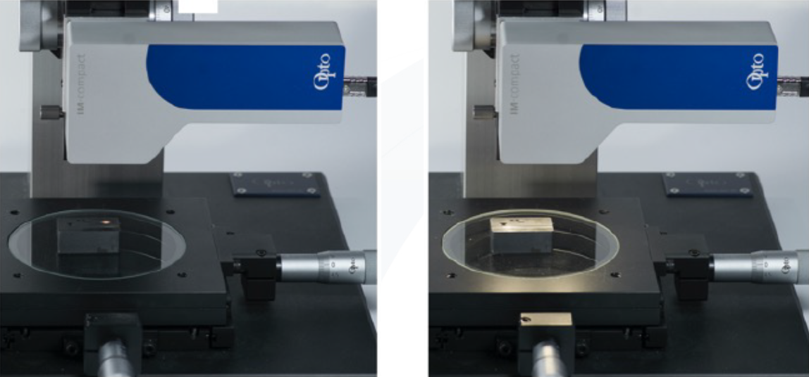
The light sources can be selected and adapted using software, as can the required camera parameters.
For defect detection, the integration of several illumination types within one sensor is ideal. Depending on the reflection behaviour of the test object, the appropriate illumination concept can be selected. In the case of machine integration, automation can also be realised via SDK.
These ground-glass samples are opaque to light and must therefore be examined in reflected light in order to detect the smallest defects and features through the interaction of the surface and the light irradiation used.
In reflected-light microscopy, a distinction is made between bright-field and dark-field illumination. In a pure digital microscope, the eyepiece is replaced by a camera chip, as in the imaging module of the compact M platform shown here.
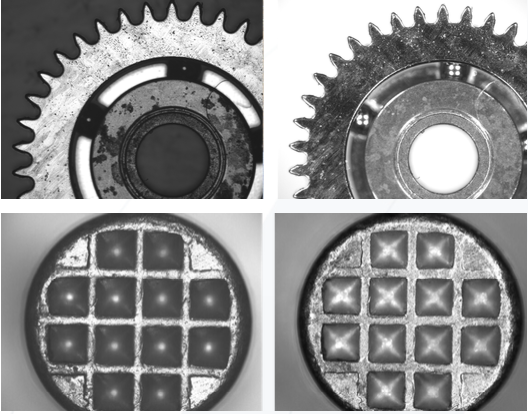
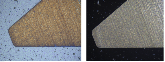
Defect identification using different illumination concepts – bright field (left) vs. dark field (right)
The standard metallic magnifications referred to in the corresponding standards are 50x, 100x, 200x, and 500x, respectively – roughly equivalent to 5x, 10x, 20x, and 50x for a digital microscope.
Despite a magnification of 3.75x, the above- mentioned Opto Imaging Module has a resolution of 1 micrometre per pixel. This hardly leads to more detailed information even with higher magnification digital microscopes – on the contrary, the result is a smaller image field. The situation is different with optical microscopes. Here, a higher magnification does indeed lead to more detail, because the eye is much better in detecting smallest differences than an image sensor.
Historically, the known standard magnifications are designed for standard microscopes. They are difficult to compare directly with digital systems. To ensure a clear comparison, one should therefore always consider the required object field as the decisive parameter. With digital imaging, criteria such as resolving power, contrast rendition, colour fidelity or the reproducibility of the measurement specifi- cations play a much greater role. A change in this
respect can also be seen in the standards of metallic image analysis. Topics or specifications such as “pixel resolution” are mentioned more and more often
Particularly for advanced evaluations with BIGDATA and machine learning with neural networks, larger image fields and repeatable data often count more than pure image quality. Here, it is important to feed the system with a lot of test data and to determine rules that are to be adapted and automated later. In digital noise, for example, there is often much more object information than is apparent to the observer at first glance. By classifying data packets, features such as structure, roughness, degree of crystallisation, hardness, toughness, colour, orientation, topography or even wear can be assigned. By means of AI, a holistic evaluation is thus realized depending on the requirement profile.
One possible application example is weld seam testing. As shown in Fig. 6, it can be used to very reliably derive or evaluate the specimen strength, penetration, bonding defects, weld build-up, through-welding or even cracking of a weld seam only by means of comparisons. The result – “IO” or “nIO”.
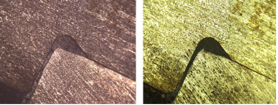
Shape, position and structure analysis – IM · bright field (left) vs. IM · dark field (right)
Effects that otherwise only occur using microscopy techniques such as differential interference contrast DIC or polarisation microscopy can be realised with a wide variety of samples thanks to the special design of an Imaging Module and can be used to determine quality.
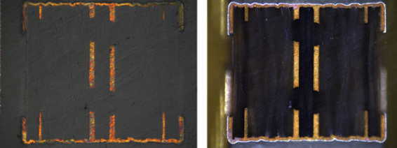
Contrast enhancement of the height structures using IM · bright field; normally only visible with DIC prisms.
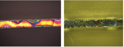
Polarisation effects provide information about internal stresses in the material
In addition to the typical images of the microstructure in the coaxial bright field, especially in the dark field (IM · ring light), impurities or the smallest scratches on the surface are shown in good contrast. Blowholes, pores or cracks are visible as white or black irregularities. For the quality control of samples or the evaluation of sample preparation, the different illumination methods, which can be easily switched via software, are of immense advantage. The colour variants of the IM · MVM series also allow structural anomalies such as copper oxide inclusions (Cu2O) to be easily recognised in image fields of approx. 2mm.
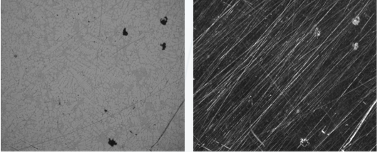
Blowhole with bright field (right) and scratch with dark field (left)
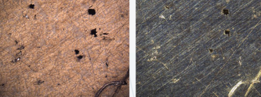
Discernible microstructure in 2mm object field
Many applications for the assessment of metals use image processing algorithms or image analysis tools. These require a well-contrasted basic image in order to automatically determine grain sizes, shape and position with defined threshold configurations. Here, the high-quality optics of the Opto Imaging Modules and the matched illumination provide high- resolution, repeatable image data.
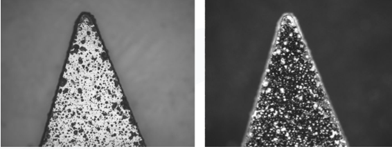
High-contrast illustrations as the basis for Image analysis
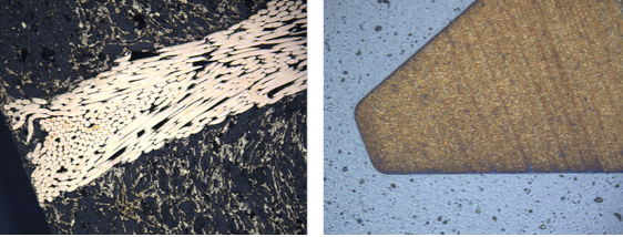
Bright field image of a crimp connection (left) & contour, grain and structure at a glance (right)
In recent years, traditional visual light microscopy has been increasingly supplemented by purely digital microscopes. Their use is also becoming increasingly important in metallography. The clear advantages are: the immediate digital availability of the images, fatigue- free inspection or the possible automation of the inspection task. In an age where data is stored and analysed in the cloud and programmes such as ‘LabView’ or ‘ImageJ’ are popular, custom codes must be written using Python or C++. Only this way allows further individual processing and analysing of the generated data.
All this requires easy handling of the microscope, a compact and robust housing, optimal matching of camera, optics and illumination as well as the right app – the concept of the MVM family of Opto Imaging Modules
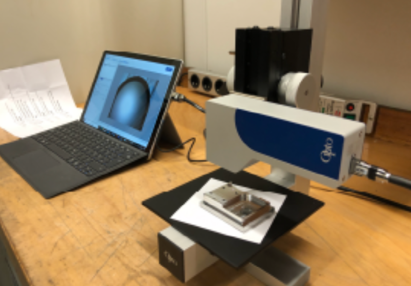
Mobile workstation with an Opto IM · MVM & accessories
Customer-Task
• Grain & Structure Analysis of Metals
• Predictive Maintenance of production processes
• Quality control of mechanical parts
• Damage evaluation of metal malfunction
Solution
• Imaging Module compact M (MVM)
• Small footprint with portable stand and case • Easy to use and free SW OptoViewer 2.0 software
• Ring- and Coaxial Illumination integrated • Direct measurement without calibration • USB one cable solution
Advantage for customer
• Pure all in one digital microscope
• Micrometer / pixel Resolution with large FoV
• High Contrast and Color stability
• Repeatability of Image
• Open SW architecture
• Easy machine integration
• Bright and Darkfield in one unit
